
japan silicon edge grinding equipment manufacturer Grasping strong production capability, advanced research strength and excellent service, Shanghai japan silicon edge grinding equipment supplier create the value and bring values to all of customers.
 WhatsApp)
Wafer marking is done with a laser, according to Semiconductor Equipment and Materials International (SEMI) Standards. Wafers after cutting have sharp edges, edge grinding is carried out to remove sharp edges. Lapping/grinding is an operation where material is removed from wafers with abrasive slurry.
SEMI Edge Profile WG Abstract A survey was designed and distributed to device manufacturers in Japan and the US in order to solicit their views on the need for a more precise characterization of the silicon wafer edge profile. It is believed that the current edge profile template
calcite grinding machine silicon carbide slag cone crushing. ... silicon ore extraction equipment . rank silicon gold mining machine ore medchal stone crusher silicon carbide israeltheadmagstone crusher silicon carbide israel rank silicon crusher stone medchal silicon cisco gold mining equipment includes gold ore machine for sale get price and ...
Indeed, NTC grinding machines used to be a subject of adoration in both the domestic and overseas markets. The mythology in these words has further evolved. Cylindrical grinding machines .
Polishing Grinding Manufacturers Wafer Production Equipment Companies involved in Polishing Grinding machine production, a key piece of equipment for the production of solar wafers. 21 Polishing Grinding equipment manufacturers are listed below.
Specialized Grinder for Sapphire and SiC ... Rokko has introduced fixedabrasivegrain type equipment to their sapphire and SiC grinding newly introduced service is now available for customer evaluations. Rokko is capable of providing process services at the same control level of the semiconductor industry that is cultivated ...
We manufacture premiere CMP, grinding and substrate manufacturing equipment for use in the production of semiconductor devices. Every piece of equipment from Revasum is designed with the customer in mind; as a result, each one meets or exceeds our customer''s performance targets.

Newlydeveloped grinding unit enhances the rotative precision of the spindle, and improves the surface roughness. The noncontact measuring method achieves the stable alignment. Performs the noncontact measuring of the preprocessed wafer thickness at multiple points, the diameter and notch depth of the postprocessed wafer.
Edge chipping of silicon wafers in diamond grinding. ... an optical microscope (MX40, Olympus, Japan) was utilized to observe edge chipping. The optical image of edge chipping was then imported into the AutoCAD software for chipping edgeprofile approximation and chipping area calculations. ... In grinding a silicon wafer by a diamond wheel ...
: Over Molding Process Development for a Stacked WLCSP (4/10) MC3 mold materials with the different package structures. The material basic properties and technique are shown in Table 2. This evaluation was done with grinding and larger 2nd chip size. The exposed chip tends to show lower warpage and the 2nd chip reduces wafer warpage.
This review paper discusses historical perspectives on grinding of silicon wafers, impacts of wafer size progression on applications of grinding in silicon wafer manufacturing, and interrelationships between grinding and two other silicon machining processes (slicing and polishing). It .
China Green Silicon Carbide Grinding Stone 4X2 Inch, Find details about China Grinding Stone, Grinding Wheel from Green Silicon Carbide Grinding Stone 4X2 Inch SIGNI INDUSTRIAL (SHANGHAI) CO., LTD.
COMPOL Silicon and Exotic Material Polish. COMPOL is a colloidal silica slurry developed especially for polishing metals, ceramics, and electronic substrates such as lithium tantalate (LiTaO3), lithium niobate (LiNbO3), and sapphire.
Wafer backgrinding, also known as Wafer thinning, is a semiconductor device fabrication step during which wafer thickness is reduced to allow for stacking and high density packaging of integrated circuits (IC).. ICs are being produced on semiconductor wafers that undergo a multitude of processing steps. Silicon wafers commonly used today are roughly 750 μm thick to ensure a maximum of ...
Since 1932 of our foundation we have been walking step by step with customers to make use of unrivaled hardness of diamond for industrial use. Through a tool I cut it and sharpen it and polish it, and to empty a hole into, we will offer solution more than the expectation of in future.|Semiconductor wafersTokyo Diamond Tools Mfg. Co., Ltd.
Grinding and Polishing GRINDING removes saw marks and levels and cleans the specimen surface. Polishing removes the artifacts of grinding but very little stock. Grinding uses fixed abrasives—the abrasive particles are bonded to the paper or platen—for .
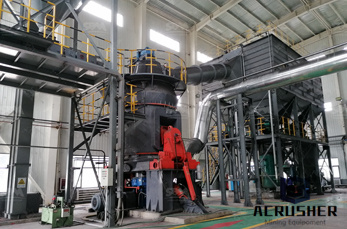
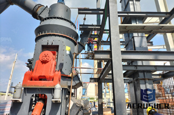
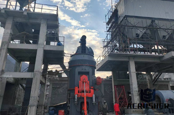
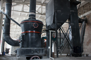
Semiconductor Manufacturing Equipment > Wafer Manufacturing System; Wafer Manufacturing System. Variety of products line for wafer manufacturers including Sliced Wafer Demounting and Cleaning Machine and Wafer Edge Grinding Machine. Sliced Wafer Demounting and .
Very hard, functions as the "cutting edge" in grinding work. Bonds and holds abrasive grains. Functions as a "chip pocket" and helps cool the grinding wheel. A grinding wheel consists of three elements: abrasive grain, bond and pore, as shown in figure 1. ... Silicon carbide abrasive grain: GC
Oct 23, 2019· Falkonry to Demonstrate Its Edge Analyzer at the Innovation Leaders Summit in Japan and the Silicon Valley New Japan Summit in California October 23, 2019 09:00 AM Eastern Daylight Time
The slanted or rounded edge between the bottom of a wafer and the side of a wafer is the bevel region. Beveling is achieved by edge grinding, or pressing the edge of a grooved grinding wheel against the wafer as it rotates. Beveling wafers can help to prevent chipping and can have an impact on the function of the semiconductor when it is finished.
surface grinding in silicon wafer manufacturing wire sawn wafer grinding, but will also briefly cover another application etched wafer grinding. Following this introduction section is a description of the surface grinding process. After that, the applications to wire
With every purchase of a qualifying STUDER grinding machine, you''ll get 5% back in StudE Bucks, budget insurance that''s good for any UNITED GRINDING North America product or service. Learn More Boost Your Manufacturing Know How with The Motion Blog
Okamoto is a leading manufacturer of precision grinding and polishing tools since 1935. Grinding tools used in applications of wafer manufacturing, SOI, TSV, MEMS, thin wafers down to 25 um, bonded wafers, bumped wafers, solar ingot grinding, quartz, sapphire, GaAs, InP and more.

Wafer Edge Grinders. Since introducing the world''s first Numeric Controlled Edge Grinder over 30 years ago, Daitron has continued to make improvements in quality and yield to the processing of Silicon and other semiconductive materials. The latest VTwin contouring technology utilizes the 2 axis vertical grinding process. This system assures ...
WhatsApp)